Friday, 15 March 2013

7 Segment Display Interfacing with 8051


INTRODUCTION: 

This post is about to interface a seven segment LED display to an 8051 microcontroller. Seven segment LED display is very popular and it’s just 7 LEDs that have been combined into one case to make a convenient device for displaying numbers and some letters. Knowledge about how to interface a seven segment display to a microcontroller is very helpful in designing embedded systems. A seven segment display consists of seven LEDs arranged in the form of a “squarish eight” slightly inclined to the right and a single LED as the dot character. Different characters can be displayed by selectively glowing the required LED segments. 

Seven segment displays are of two types, 

Common Cathode: In this method, all segment share common cathode. 

Common Anode: In this method, all segment share common anode. 

Here common anode seven segment display is used because the output current of the microcontroller is not sufficient enough to drive the LED’s. In order to turn ON a segment the corresponding pin must be set to 0 and to turn it OFF it is set to 1. 


A resistor is required to limit the current. Rather than using a resistor from each LED to ground, you can just use one resistor from Vcc to pin 3 (‘com’) to limit the current. 

DIGIT DRIVE PATTERN

Digit drive pattern of a seven segment LED display is simply the different logic combinations of its seven segment terminals ‘a’ to ‘h’ in order to display different digits and characters. The common patterns (0 to 9) of a seven segment display are shown in the table below. 


CIRCUIT DIAGRAM


INTERFACING CODE

// Programming for interfacing of Seven Segment Display to 8051 

#include<reg51.h> 

delay_ms(int time) // Time delay function 
int i,j; 
for(i=0;i<time;i++) 
for(j=0;j<1275;j++); 
void main() 
char num[]={0x40,0xF9,0x24,0x30,0x19,0x12,0x02,0xF8,0x00,0x10}; 
// Hex values corresponding to digits 0 to 9 
int s; 
while(1) 
    { 
    for(s=0;s<10;s++) 
        { 
          P2=num[s]; 
         delay_ms(200); 
        } 
    } 
}

Wednesday, 13 March 2013

LED Interfacing with 8051

-->

LED (LIGHT EMITTING DIODE) 

Light Emitting Diodes (LED) is the most commonly used electronic components, generally for display digital states. Typical uses of LEDs include alarm devices, timers and confirmation of user input such as a mouse click or keystroke, events etc. LEDs are very cheap and easily available in a variety of shape, size and colors. 

OPERATION OF LED: 

The principle of operation of LEDs is simple. 

When using an LED you must use a resistor to limit the current flow. If you just connect an LED directly to a pin of the micro controller you run the risk of damaging the micro controller by allowing too much current flow into or out of the pin. 

You have to be aware of the current limits for the pin at which you are going to connect LED. A port current limit is the total current flowing from a number of individual pins. 

Sinking (power flow into the pin) and sourcing (power flow out of the pin) may have slightly different current limits so you have to check the data sheet for the exact values. 

You can use 10-15 mA as a safe LED current which will provide decent light intensity and conserve battery power. 

Determine the Series resistor using Ohms law with an excess voltage value and current value for LED. 

Red LED's generally need 1.5V to 1.9V to light any extra voltage must be dropped with a series resistor else the LED will draw extra current in an attempt to lower the supply voltage down to the 1.5V level. 

The typical supply voltage is 5V. Then, 5 - 1.7 = 3.3V of excess voltage. 

Let’s design the LED to use 10mA 

Ohms law Resistance R = V / I 

3.3 / 10mA = 330 Ohms, Place a 330 ohm resistor in series with the LED. 

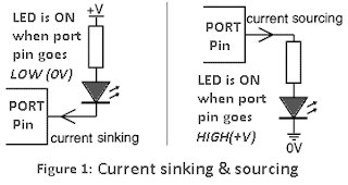
You can connect the LED and its resistor in one of two ways: 


Sinking Current where the LED is connected to Positive power and the pin on the micro goes low to ground potential to light the LED. 

Sourcing Current the LED is connected to ground and the Pin on the micro controller goes HIGH to positive voltage to light the LED.

CIRCUIT DIAGRAM:


INTERFACING CODE:

             // Program to blink the LEDs (LEDs are connected to port 2)

#include<reg51.h>

void delay(int time)                               //This function produces a delay in msec.
{
int j,k;
for(j=0;j<time;j++)
for(k=0;k<1275;k++);
}
void main()
{
   while(1)
      {
        P2=0x00;
       delay(30);
       P2=0xff;
       delay(30);
      }
}
-->

Monday, 11 March 2013

AT Commands for GSM SIM 300 Interfacing


AT Commands are Instructions and used for control a Modem. Every command line start with "AT". That's why modem commands are called AT commands.
This article describes the AT commands for reading, sending and deleting SMS and also receiving, dialing, hanging a CALL from the SIM300 GSM modem inbox. You can also check the balance in sim card in SIM300.

Setup testing procedure for AT commands:

  • Insert the SIMCARD into SIM Tray
  • Connect the RS232 cable to the PC serial port (DB-9)
  • Open hyper terminal from windows 
  • Select the COM port with baud rate 9600 
  • Type AT commands and press enter and you will get OK; that means communication is OK.

Reading a SMS from the Inbox:

AT+CMGF=1 then press enter
AT+CMGR= no. and press enter; Number (no.) is the message index number stored in the SIM card.
The modem will reply with the text of the first SMS in the inbox along with sender’s mobile number, date and time.

Sending SMS from SIM300:

AT+CMGF=1 press enter
AT+CMGS=”mobile number” press enter
Once The AT commands is given’ >’ prompt will be displayed on the screen.
Type the message to send via SMS. After this, press ctrl+Z to send the SMS.
If the SMS sending is successful, “ok” will be displayed along with the message number.

Deleting a SMS from inbox:

  • To delete the first message from the inbox type the command AT+CMGD=1 and press enter; the modem will delete the first message in the inbox. 
  • To delete the second message from the inbox type the command AT+CMGD=2 and press enter; the modem will delete the second message in the inbox …..and so on. 

Receiving an incoming Call:

To receive a ringing call, type the command ATA and press enter

Dialing a new number from SIM300:

To call to a number send the command ATD followed by the mobile number
For example, to call the mobile number 9928142466 send the command as, ATD9928142466; and press enter

Hanging up a call:

To hang up a ringing call or a call in progress type the command ATH and press enter

How to check a balance in SIM300?

To check a balance in your simcard in SIM300 type the command ATD followed by your service provider balance checking number; For example to check balance for Airtel or BSNL; type ATD*123# and press enter, You will get your simcard balance with expire date.


Interfacing 16x2 LCD with 8051

-->

LCD display is an inevitable part in almost all embedded applications and this article is about interfacing 16×2 LCD with 8051 Microcontroller. Many guys find it hard to interface LCD module with the 8051 but the fact is that if you learn it properly, it’s a very easy job and by knowing it you can easily design embedded display applications. Thoroughly going through this article will make you able to display any text (including the extended characters) on any part of the 16×2 display screen. In order to understand the interfacing first you have to know about the LCD.


What is 16×2 LCD Module?

16×2 LCD module is a very common type of LCD module that is used in 8051 based embedded applications. It consists of 16 rows and 2 columns of 5×7 or 5×8 LCD dot matrices. The module were are talking about here is type number JHD 162A which is a very popular one. It is available in a 16 pin package with back light, contrast adjustment function and each dot matrix has 5×8 dot resolution. The pin numbers, their name and corresponding functions are shown in the table below. 

Pin No. Name  Function
  1.   Vss        This pin must be connected to the ground 
  2.   VCC       Positive supply voltage pin (+5V DC) 
  3.   VEE       Contrast adjustment 
  4.   RS         Register selection 
  5.   R/W       Read or write 
  6.   E           Enable 
  7.   DB0       Data 
  8.   DB1       Data 
  9.   DB2       Data 
  10.   DB3       Data 
  11.   DB4       Data 
  12.   DB5       Data 
  13.   DB6       Data 
  14.   DB7       Data 
  15.   LED+     Back light LED+ 
  16.   LED-      Back light LED- 
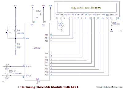
VEE pin is meant for adjusting the contrast of the LCD display and the contrast can be adjusted by varying the voltage at this pin. This is done by connecting one end of a POT to the Vcc (5V), other end to the Ground and connecting the center terminal (wiper) of the POT to the VEE pin. See the circuit diagram for better understanding.

The JHD 162A has two built in registers namely data register and command register. Data register is for placing the data to be displayed, and the command register is to place the commands. The 16×2 LCD module has a set of commands each meant for doing a particular job with the display. We will discuss in detail about the commands later. High logic at the RS pin will select the data register and Low logic at the RS pin will select the command register. If we make the RS pin high and the put a data in the 8 bit data line (DB0 to DB7), the LCD module will recognize it as a data to be displayed. If we make RS pin low and put a data on the data line, the module will recognize it as a command. 

R/W pin is meant for selecting between read and write modes. High level at this pin enables read mode and low level at this pin enables write mode.

E pin is for enabling the module. A high to low transition at this pin will enable the module. 

DB0 to DB7 are the data pins. The data to be displayed and the command instructions are placed on these pins. 

LED+ is the anode of the back light LED and this pin must be connected to Vcc through a suitable series current limiting resistor. LED- is the cathode of the back light LED and this pin must be connected to ground. 


What is 16×2 LCD Commands? 

16×2 LCD module has a set of preset command instructions. Each command will make the module to do a particular task. The commonly used commands and their function are given in the table below. 

LCD Command Function 

0F      LCD ON, Cursor ON, Cursor blinking ON 
01      Clear screen 
2         Return home 
4         Decrement cursor 
06       Increment cursor 
E        Display ON, Cursor ON 
80       Force cursor to the beginning of 1st line 
C0      Force cursor to the beginning of 2nd line 
38      Use 2 lines and 5×7 matrix 
83      Cursor line 1 position 3 
3C     Activate second line 
0C3    Jump to second line, position3 
OC1   Jump to second line, position1 


LCD initialization 

The steps that have to be done for initializing the LCD display is given below and these steps are common for almost all applications. 
  • Send 38H to the 8 bit data line for initialization
  • Send 0FH for making LCD ON, cursor ON and cursor blinking ON.
  • Send 06H for incrementing cursor position.
  • Send 01H for clearing the display and return the cursor.

Sending data to the LCD 

The step for sending data to the LCD module is given below. I have already said that the LCD module has pins namely RS, R/W and E. It is the logic state of these pins that make the module to determine whether a given data input is a command or data to be displayed. 
  • Make R/W low.
  • Make RS=0 if data byte is a command and make RS=1 if the data byte is a data to be displayed.
  • Place data byte on the data register.
  • Pulse E from high to low.
  • Repeat above steps for sending another data.

Circuit


The circuit diagram given above shows how to interface a 16×2 LCD module with AT89S1 microcontroller. Capacitor C3, resistor R3 and push button switch S1 forms the reset circuitry. Ceramic capacitors C1, C2 and crystal X1 is related to the clock circuitry which produces the system clock frequency. P1.0 to P1.7 pins of the microcontroller is connected to the DB0 to DB7 pins of the module respectively and through this route the data goes to the LCD module. P3.3, P3.4 and P3.5 are connected to the E, R/W, RS pins of the microcontroller and through this route the control signals are transferred to the LCD module. Resistor R1 limits the current through the back light LED and so do the back light intensity. POT R2 is used for adjusting the contrast of the display. 


Assembly Program 

MOV A,#38H // Use 2 lines and 5x7 matrix 
ACALL CMND 
MOV A,#0FH // LCD ON, cursor ON, cursor blinking ON 
ACALL CMND 
MOV A,#01H //Clear screen 
ACALL CMND 
MOV A,#06H //Increment cursor 
ACALL CMND 
MOV A,#82H //Cursor line one , position 2 
ACALL CMND 
MOV A,#3CH //Activate second line 
ACALL CMND 
MOV A,#49D 
ACALL DISP 
MOV A,#54D 
ACALL DISP 
MOV A,#88D 
ACALL DISP 
MOV A,#50D 
ACALL DISP 
MOV A,#32D 
ACALL DISP 
MOV A,#76D 
ACALL DISP 
MOV A,#67D 
ACALL DISP 
MOV A,#68D 
ACALL DISP 
MOV A,#0C1H //Jump to second line, position 1 
ACALL CMND 
MOV A,#67D 
ACALL DISP 
MOV A,#73D 
ACALL DISP 
MOV A,#82D 
ACALL DISP 
MOV A,#67D 
ACALL DISP 
MOV A,#85D 
ACALL DISP 
MOV A,#73D 
ACALL DISP 
MOV A,#84D 
ACALL DISP 
MOV A,#83D 
ACALL DISP 
MOV A,#84D 
ACALL DISP 
MOV A,#79D 
ACALL DISP 
MOV A,#68D 
ACALL DISP 
MOV A,#65D 
ACALL DISP 
MOV A,#89D 
ACALL DISP 
HERE: SJMP HERE 
CMND: MOV P1, A 
CLR P3.5 
CLR P3.4 
SETB P3.3 
CLR P3.3 
ACALL DELY 
RET; 
DISP: MOV P1, A 
SETB P3.5 
CLR P3.4 
SETB P3.3 
CLR P3.3 
ACALL DELY 
RET; 
DELY: CLR P3.3 
CLR P3.5 
SETB P3.4 
MOV P1, #0FFh 
SETB P3.3 
MOV A, P1 
JB ACC.7, DELY 
CLR P3.3 
CLR P3.4 
RET; 
END

Subroutine CMND sets the logic of the RS, R/W, E pins of the LCD module so that the module recognizes the input data (given to DB0 to DB7) as a command. 

Subroutine DISP sets the logic of the RS, R/W, E pins of the module so that the module recognizes the input data as a data to be displayed.
-->

Sunday, 10 March 2013

What is PCB (Printed Circuit Board) ?

-->
Definition:
A PCB is a Printed Circuit Board, and used to mechanically support and electrically connect electronic components using conductive pathways (copper traces), signal traces etched from copper sheets laminated onto a non-conductive substrate Glass Epoxy (FR4).

Also PCBs are a composite of organic and/or inorganic dielectric materials with many layers with wiring interconnects and also house components like inductors and capacitors. There isn’t any standard printed circuit board as such and each board is unique, often a function of the product itself.

PCB Design Layers:


A PCB design package allows the designer to define and design on multiple layers.

Many of these are physical layers such as:
• Signal Layer
• Power plane Layer
• Mechanical Layer

And some are special layers such as:
• Solder & Paste Mask Layers
• Silkscreen or Top Overlay Layers
• Drill guides
• Keep-out Layer

Types of PCB:

A PCB can be of four types: Rigid board , Flexible board and Rigid-flex board, Metal-core and Injection Molded boards out of which the Rigid board is the most popular. Further these may be Single Sided, Double Sided or Multilayer. 
The mechanical, electrical, chemical and thermal properties of the material should be considered while making PCBs otherwise the reliability of the board suffers. Presently, copper-clad laminates of different reinforced resin systems are used in rigid boards. Examples include Fire resistant FR-4 epoxies, PTFE, cyanate esters, polymides etc. Most commonly used reinforcement material is continuous filament E-Glass. Flexible and rigid flex-boards have random arrangements of conductors on a flexible base and may be with/without cover layers. Here, the wiring is restricted to select areas of the plane. In case of constraining metal core technology, the PCB can be of standard materials but the core materials must have low Coefficient of Thermal Expansion and strength to constrain the PCB. Copper-Invar-Copper and Copper-Molybdenum-Copper are two popular materials for this purpose. Molded boards have resins containing fillers which are molded into a die to form the required shapes.

What is PCB Board Design?


  • PCB board design defines the electrical pathways between components
  • It is derived from a schematic representation of the circuit
  • When it is derived, or imported from a schematic design, it translates the schematic symbols and libraries into physical components and connections


PCB Manufacturing Process:


Step 1: Film Generation

The film is generated from the design files (Gerber/CAM files) which are sent to the manufacturing house. One film is generated per layer

Step 2: Raw Material

Industry standard 0.059” thick, copper clad panel

Step 3: Drill Holes

Using NC machines and carbide drills to drill holes according to the drill spec sent to the manufacturing house

Step 4: Electroless Copper

Apply thin copper deposit in hole barrels

Step 5: Apply Image

Apply photosensitive dry film to panel and use a light source and the film to expose the panel

Step 6: Pattern Plate

Electrochemical process to build copper in the holes and on the trace areas. Apply tin to surface

Step 7: Strip and Etch

Remove the dry film, and then etch the exposed copper. The tin protects the copper circuitry from being etched away

Step 8: Solder Mask

Apply a solder mask area to the entire board with the exception of solder pads

Step 9: Solder Coating

Apply solder to pads by immersing into tank of solder. Hot air knives level the solder when removed from the tank

Step 10: Nomenclature(Silk Screen Printing)

Apply white letter markings using screen printing process
-->

In System Programming


For embedded system application you have a dedicated intelligent semiconductor chip which is capable to execute a software program, and behave at input and output data pins as per software instructions. These chips are called a processor and a processor can be microcontroller, microprocessor, DSP, etc. 
The software for such embedded system processor generally is written in the laptop or PC, compiled (or assembled) using a cross-compiler tool (called cross compiler because program is written in PC and executed in embedded processor). Compiler (or assembler) generate executable file for the particular processor and this program should be inserted (saved) in processor's non-volatile memory (internal or external). 


Programming the processors's nonvolatile memory is itself a tough task. In earlier days practice was to remove processors or its external memory from target board and place it in a specific programming device. Even today many people program processor in same way. But a new and convenient way is to program the processor or its memory while remaining in the target board. It is called in system programming. 

What you need for in system programming?

  1. Hardware interface from you PC, so that the executable program can be transferred from PC / Laptop. This interface can be DB-9 connector, USB or parallel (printer) port. 
  2. Software running in the PC which can control the data sending on hardware interface port. Generally this software are Flash tools like Flash magic, or IDEs like TI's code composer studio, Microchip's MPLAB, etc
  3. A specific hardware which would recieve data from the PC and transfer it to target board using a special hardware interface like SPI (serial programming interface), JTAG, Microchip's ICD, etc. Here JTAG and ICD have additional capability for debugging. 
  4. Sometime, the hardware interface mentioned in last point is not used. But the target processor itself have BOOTLOADER software programmed or pre-programmed in it. Bootloader is a software in the program memory executes when processor resets. It give use a option to either run the existing application software or receive a new application software from PC using a serial interface. Generally PC transfer data using RS-232 (DB-9 connector) and MAX 232 IC convert it to UART (Rx, Tx) data. This self programming capablity using boot loader provides excellent convenience and low cost. But it need a boot loader in the processor and UART compability.

Wednesday, 27 February 2013

Magnetic Core - Inductors and Transformers

Motivation

For realizing any practical embedded system use of Magnetics (Inductors and Transformers) are unavoidable as it is a integral part of SMPS required for control supply. In other words I can also say selecting or making Magnetics is more critical and time consuming part of complete SMPS realization. To design transformers and Inductor, we will have a short overview of magnetic cores. 


What is a Magnetic Cores?

Magnetic cores are basically a piece of magnetic material made in a particular shape. This magnetic material provide low reluctance path to magnetic flux. (Here is word reluctance for magnetic flux is similar to resistance for electric current. That is lesser the reluctance more is the flux. Air itself have very high reluctance.) 

These low reluctance magnetic cores provide low reluctance path hence guide the flux in particular path. Confining magnetic flux in particular path solve one two or both purposes. 

1. Coupling electrical coils wounded around the path i.e. on the core. By using this magnetically coupled link, the coils can exchange the electrical energy. This is a typical application of Transformers. Please refer the image blow: 


2. Storing controlled amount of energy in the magnetic flux. This is a typical application of Inductors. Inductor cores generally have gaps, either a intentionally given small air gap e.g. gaped ferrite cores (please see image below), or distributed gap like in iron dust powder cores. 


TYPES


Laminated Core

These are made up by staking thin lamination of Iron material. These cores can carry high magnetic flux density without getting saturated, but operating frequencies are quite low (as high core losses occurs at high frequency). Generally used on power frequencies (50 Hz in India)  Almost all power transformers are makeup of Laminated cores. 

Ferrite Cores 

These are made of Ferrite material in many difference shapes (EE, EI, RM, Toroids, etc). Below image shows ferrite cores of EE shape. 


These are having low saturation flux density typically 0.2 web/m^2. Because of having very low core losses, it can be operated at very high switching speeds i.e. hundreds of kHz. These are used as Inductor with a small gap in the magnetic path, or as a part of high frequency transformer with no gap. Some application like Flyback converter needs a transformer with primary winding working as a Inductor also. In such case also a gaped ferrite core is used. 

Powder Cores

Power cores are made of Iron powder dust and are mostly available in Toroidal shape. It have mixture of magnetic material and non magnetic materials. Therefore, there would be evenly distributed gap between magnetic grain. These core are used in the Inductor application generally required in DC to DC converters and SMPS application. 

Tuesday, 26 February 2013

GPS / GSM Based Vehicle Tracking System


INTRODUCTION

The number of vehicles is increasing at a sharp rate, and the vehicle's dispatch and safety management has become an important problem of the department of the traffic. Therefore, the demand for a system with function of positioning and monitoring rises as well. The intelligent vehicle monitoring system, based on the GPS/GSM, integtes the technology of GPS, GIS and modern commutation technologies into the monitor and management of the vehicles. With the exchange of the system information, we can not only obtain the information of trip vehicles and road blocs that are needed for decision-making in traffic engineering, bnt also can meet the demand for vehicle guards against theft, alarm and help-seeking which greatly improves the transportation efficiency and ensures traffic safety. 


ANALYSIS OF INTELLIGENT VEHICLE MONITORING AND POSITIONING SYSTEM

A intelligent vehicle monitoring and positioning system is made number of vehicle terminal, wireless communication link and vehicle monitor management center  The wireless communication link of the system can adopt tanking system, GSM network or other wireless transmission systems to achieve data transmission. The monitor management center is made up of dispatch terminal, alarm terminal, data acquisition terminal (pre-positive machine) or network communication server, dispatch statistic printing terminal and electronic map showing terminal, which make up a LAN structure. In order to realize such functions as the management and dispatch of the vehicle, all the terminals can be incorporated together in terms of the need of the work. 

Technology of Vehicle Unit's Positioning
The vehicle unit of the intelligent vehicle monitor and positioning system is made nip of the position-getting unit, wireless communication module and controlling unit. In the vehicle unit, the function of the position-getting unit is to get the position of the vehicle automatically. It is an important index for vehicle unit's function and performance that whether the vehicle unit can get the current position of the vehicle accurately and quickly  The position-getting module of the vehicle unit involves the automatic positioning technology. There are many kinds of technologies that can be used in the vehicle terminal, such as the GPS technology, the GLONASS technology, GSM cell phone positioning technology and the BEIDOUXING positioning technology. The precision and the application fields of all the positioning technologies are shown in the table below.


From table 1, the GPS technology can be found out that it is the most extensive used in the vehicle monitoring and navigation. The basic principle of the GPS pseudo-range positioning is: The satellites send their own ephemeris indexes and time information. The GPS receiver can get several pseudo-range equations in its observation range by receiving several satellites (usually four). By applying the satellite ephemeris data to these equations, three dimensional position and direction speeds of movement and time information can be obtained by the receiver. The GPS pseudo-range positioning principle sketch is as shown in figure below. 


Wireless Transmission Method of Intelligent Vehicle Monitoring System

With the development of electronics, computer science and information technology, the development of the communication system has experienced vast changes, from wire communication to wireless communication  from voice transmission to data transmission, from local area to wider areas, etc. There are many communication networks and methods that can be used in the intelligent vehicle monitor and positioning system. the applied communication manners can be sum up as follows: routine communication manner, trunking communication, GSM, GPRS and satellite communication. Different application chooses different modes of wireless communication according to the actual demand.

Based on the GSM network that owns the digital mobile cellular communication technology, the reliability can be assured in the vehicle monitor and positioning system. Short message is a kind of convenient data communication manner of GSM. Short messages of GSM will be used as the communication method of the vehicle monitor and positioning system.


DESIGN SCHEME OF GPS/GSM VEHICLE MONITORING SYSTEM

Firstly, transmitting the mobile object's information such as the dynamic position (including longitude and latitude), time, state and so on through wireless communication link to the monitoring center real-timely; Secondly, showing the position and the moving track of the mobile object on the electronic map with the strong geographical information inquiry function; Thirdly, monitoring and inquiring the information of the speed, moving direction and vehicle state of the object that users are interested in, which provides the visual foundation for dispatch. This improves the operation efficiency of the vehicle and ensures the safety of vehicle. It is especially suitable for such departments as bus service, taxi, public security, bank, insurance, airport, etc. to monitor and dispatch vehicles.

Principle of GPS/GSM Vehicle Monitoring System

Making full use of GIS, GPS and GSM technology, the vehicle monitoring system based on GPS/GSM is a computer network system developed for real-time vehicle surveillance. The positioning terminal on the monitoring object receives the positioning data from the GPS satellites (24 satellites distributed on 6 diffident earth tracks) every second by GPS module and calculates its own geographical coordinates with the data from three or more satellites. According to the established protocols, the coordinate data which include the position and the state of the vehicle are sent to GSM network in form of short message by GSM module. The GSM network transfers the received information to the communication gateway of the monitoring center. After proper handling, the information is transmitted to the GIS monitoring terminal. In this way the monitoring center can grasp detailed real-time vehicle information. When a vehicle encounters emergency, the police can be called by positioning terminal, sending the information such as the location of the vehicle, alarm type to the monitoring center. Once the information is processed, the location of the alarm vehicle can be accurately showed on the electronic map.

The principle sketch of the vehicle monitoring system based on GPS/GSM is shown in the figure below.


Design of work Structure of GPS / GSM Intelligent vehicle Monitoring System

The GPS/GSM vehicle monitoring system is made up of three major parts: monitoring and commanding center, GSM communication (including communication control machine, GSM transmission module, GSM network and corresponding wire transmission) and vehicle unit. The overall structure of the vehicle monitoring system of GPS/GSM is shown in Figure blow. 


The monitoring and commanding center consists of the communication monitoring computers, GIS monitoring terminals and other computers, which are combined by network links. The communication between communication severs and GSM network adopts the DDN special line or the wireless MODEM depending on their availability. If the monitoring objects are large in number and the communication condition permits, the DDN special line can be adopted. In this way, the communication is rapid and messages are seldom congested.

DESIGN OF MONITORING AND COMMANDING CENTER

The monitoring ad commanding center is composed of communication monitoring computers, GIS monitoring terminals, GPS database sever and database backup sever through network link. The location and state information of the mobile center are sent to vehicle monitoring and managing center by means of short message through GSM network. After analyzing the location information of vehicle, the vehicle monitoring and managing center will show the moving object dynamically on the electronic map. If the vehicle meets unexpected (stolen, robbing) situations, after receiving the alarm from vehicle, the vehicle monitoring and managing center will inform the users to take relevant measures through the form of sound or light to minimize their loss. The network structure of the vehicle monitoring and commanding center is as shown in figure below. 


DESIGN OF VEHICLE UNIT

The vehicle unit is installed on the vehicle and other mobile devices. It is constituted by GPS receiver,  antenna, processing unit, GSM module and hand-free devices. GPS receiver demodulates positioning data of GPS satellites through the aerial, the process unit receives data from serial port, and the data is sent to message center after modulated. The alarm function is used in the condition that the vehicle or mobile device breaks down or pre-warns, and then the driver can press down the hidden alarm button to call the police, or is catenated with the vehicle alarm, and sends out warning information automatically. The alarm information includes the number, the state, and the location of the vehicle. The dispatch center will take relevant reactions after receiving the alarm. The structure sketch of the GPS/GSM vehicle unit is as shown in figure below. 


DESIGN OF COMMUNICATION GATEWAY

The communication gateway of the vehicle monitoring system is responsible for bidirectional information transmission between monitoring platform and the vehicle unit. The communication gateway comprises two parts: one is installed in the communication sever (COM SEVER): the other is installed on the communication client (COM CLIENT). The software of the communication gateway can be realized by using Visual C++. There are two processes in the communication sever: one is PROCESS GSM which is required to changing short messages into a uniform format, storing it in the short message queue temporarily waiting for inquiry of
COMM CLIENT; the other process is PROCESS CLIENT, which is used to monitor the inqiwry command of COMM-CLIENT, returning the short messages in the same format, at the same time receiving the monitoring command from the COMM-CLIENT and sending the message to vehicle unit with the DDN special line or wireless MODEM communication protocol by GSM network. The COMM CLIENT is suggested to design into a dynamic link library, with the following functions: judging whether there is short message needed, receiving short message, sending short message command.


FUNCTIONAL REALIZATION OF GPS / GSM VEHICLE MONITORING SYSTEM

1) Vehicle real-time monitoring
The information of the vehicle track and state can be shown on the electronic map in the dispatching center,
insuring the dispatching center to monitor the vehicle real timely.

2) Track playback
The location record of a vehicle, the received information of a vehicle and the alarm information in a period, etc. can be inquired at any time. And can select the position record in some time of a vehicle and carry on the track playback.

3) Road matching
According to longitude, latitude, moving direction, moving speed of the object and the road information on the electronic map, shows the vehicle object in the center of the road.

4) Routine choices
The system may provides routine choices for different conditions.

5) Voice link
The system allows two-way voice-communication when transmitting the position information of the vehicle.

6) Information inquiries
Users can real-timely inquire the information of the location of authorized vehicle and state, etc.

7)Acceptation of active alarm
When a vehicle is robbed or thieved, the vehicle terminal will send the alarm information to the center. The watcher will be noticed at the monitoring terminal through voice or ray, and the data such as the location of the vehicle (X, Y coordinate), the time of moving object will be shown on the screen. The decision of the accident will be offered for the vehicle manager. For the safety of the vehicle, on receiving the alarm information from the vehicle, the monitoring center will send the alarm information to the owner of the vehicle, noticing that the vehicle meets accident, and the owner will be supposed to take relevant actions.

8) Acceptation of stolen alarm
When the door of vehicle is prized illegally, the vehicle terminal will send the stolen alarm to the center. The
watcher will be noticed at the monitor terminal through voice or ray, and the data such as the location of the v-chicle (X, Y coordinate); time of moving object will be shown in the screen. The decision foundation of the accident will be offered to the vehicle manager. For the safety of the vehicle, on receiving the alarm information from the vehicle, the monitoring center will send the alarm information to the owner of the vehicle, noticing that the vehicle meets accident, and the owner will take relevant actions.

9) The special incident alarm
Whee met the special incident, the monitoring center will be alarmed, and the location of the vehicle will be signed with special signal. After sending the alarm information to center. the watcher will be noticed at the monitoring terminal through voice or ray, and on the electronic map the object will be signed with fresh color and special icon. The owner data will be shown in the character monitoring platform, including the number of the vehicle, license number of the vehicle, the vehicle type, the vehicle color, the motor number, using type, driver's name the license number of the driver, the department of the vehicle, the director, the telephone number, the location (X, Y coordinate), the speed, the type of the alarm and time, to help the watcher deal with alarm. The system can provide the alarm condition acceptation window for the watcher to record the acceptation condition.

10) The communication function of TCP/IP
The GIS monitoring and managing center may make communication connection through TCP/IP protocol and communication gateway to realize the monitoring and dispatching of the vehicle positioning terminal .


REFERENCES: 

Qiang Liu; Huapu Lu; Hongliang Zhang; Bo Zou; , "Research and Design of Intelligent Vehicle Monitoring System Based on GPS/GSM," ITS Telecommunications Proceedings, 2006 6th International Conference on , vol., no., pp.1267-1270, June 2006

What is RFID?


Radio frequency identification (RFID) has been around for decades. Only recently, however, has the convergence of lower cost and increased capabilities made businesses take a hard look at what RFID can do for them.A major push came when retailing giant Wal-Mart dramatically announced that it would require its top 100 suppliers to supply RFID-enabled shipments by January 2005. Though the bottom line story of that deployment has yet to surface.

Following obvious questions will strike on anybody's mind:

• What is RFID, and how does it work? 
• What are some applications of RFID? 
• What are some challenges and problems in RFID technology and implementation?
• How have some organizations implemented RFID?

TECHNICAL OVERVIEW
The basic premise behind RFID systems is that you mark items with tags. These tags contain transponders that emit messages readable by specialized RFID readers. Most RFID tags store some sort of identification number; for example a customer number or product SKU (stock-keeping unit) code. A reader retrieves information about the ID number from a database, and acts upon it accordingly. RFID tags can also contain writable memory,which can store information for transfer to various RFID readers in different locations. This information can track the movement of the tagged item,making that information available to each reader.

RFID tags fall into two general categories, active and passive, depending on their source of electrical power.Active RFID tags contain their own power source, usually an on-board battery. Passive tags obtain power from the signal of an external reader. RFID readers also come in active and passive varieties, depending on the type of tag they read. 

Active tags transmit a stronger signal, and readers can access them from further away.The on-board RFID offers tantalizing benefits for supply chain management, inventory control, and many other applications. Power source makes them larger and more expensive, so active RFID systems typically work best on large items tracked over long distances. Low-power active tags are usually slightly larger than a deck of playing cards.Active tags can remain dormant until they come in range of a receiver or can constantly broadcast a signal. Because of their on-board power source,active tags operate at higher frequencies—commonly 455 MHz,2.45 GHz, or 5.8 GHz—depending on the application’s read range and memory requirements.Readers can communicate with active RFID tags across 20 to 100 meters.

Passive tags, on the other hand, are very inexpensive; they can cost as little as 20 cents apiece, and new technologies are constantly making them cheaper to integrate into common materials and products.Because passive tags are inexpensive, they will likely be the basis of most of the growth in RFID implementations. In addition to their low cost, passive tags can also be quite small. Current antenna technology limits the smallest useful passive tag to about the size of a quarter. The larger the tag, the larger the read range. Currently, passive RFID tags contain about 2 Kbits of memory. This is too small to hold much more complex information than identification and history information. The technology behind RFID is constantly improving, so the amount of information and capabilities of RFID tags will increase over time, allowing RFID tags to eventually contain and transmit much more information. A passive-tag reader can constantly broadcast its signal or broadcast it on demand. 

When a tag comes within the reader’s range, it receives an electromagnetic signal from the reader through the tag’s antenna. The tag then stores the energy from the signal  in an on-board capacitor, a process called inductive coupling.When the capacitor has built up enough charge, it can power the RFID tag’s circuitry, which transmits a modulated signal to the reader. That return signal contains the information stored in the tag. The communication between the reader and passive tag uses one of two methods to modulate the ID signal. 

In low-frequency (less than 100 MHz) tags pass information by releasing energy from the capacitor to the tag coils in varying strengths over time, which affects the radio frequency emitted by the tag. The reader detects these varying waves and can use these variances to demodulate the code. Figure below shows this load modulation.


In higher-frequency (greater than 100 MHz) tags,the tag transmits the signal using back scatter, in which the tag’s circuit changes the resistance of the tag’s antenna. This change in resistance causes a transmission of RF waves, which the reader can pick up and demodulate. Passive tags typically operate at frequencies of 128 KHz,13.6 MHz,915 MHz, or 2.45 GHz, and have read ranges of a few inches to 30 feet. Frequency choice depends on the system’s environment,what material the signal must travel through, and the system’s required read range.

RFID tags can be encased in many materials.Plastics are a very common material for RFID, forming  identification cards for building access,credit cards,or bus fares.Tags can also go on the back of labels printed on standard ink jet printers, for placement on inventory.

STANDARDS:
Several RFID standards exist, and their applications are under debate within the RFID development community. These standards cover: 
• identification, the coding of unique item identifiers, or other data on the RF tag;
• data and system protocols, effectively the middleware of an RFID system;
• the air interface, that is, the wireless communication between the reader and the tag;
• application support, which provides advice about how to implement the technology;
• testing, compliance, and health and safety, that is, the rules that govern RFID operations; and
• terminology.

The International Standards Organization (ISO) has three standards for RFID: ISO 14443 (for contactless systems), ISO 15693 (for vicinity systems, such as ID badges), and ISO 18000 (to specify the air interface for a variety of RFID applications). A not-for-profit organization, EPCglobal, has developed a widely accepted standard for product identification. The Electronic Product Code (EPC) standard covers the air interfaces, the format for the product identification data stored in an RFID tag, and the middleware and databases storing information about the tags.

APPLICATION:
RFID applications are numerous and far reaching. The most interesting and widely used applications include those for supply chain management,security,and the tracking of important objects and personnel. Supply chain management In supply chain management, RFID tags are used to track products throughout the supply chain—from supplier delivery, to warehouse stock and point of sale. New applications target tracking from checkout through customer billing. A central database records product movement, which manufacturers or retailers can later query for location, delivery confirmation, or theft prevention. For this application, RFID basically serves as a replacement for the bar code scanners used to track products and shipments in similar ways.

Security and personal identification applications are a major and broad application of RFID. A common use of RFID is in identification cards to control building access. Many organizations use RFID tags embedded in ID cards, which are readable at a building entrance. On a similar note,some credit cards use RFID tags. Other cards use tags for automatic fare payment in mass-transit systems, such as the SmarTrip card for the Washington DC area subway and bus system (http://www.wmata.com/riding/smartrip.cfm). Essentially,these are a replacement for identification cards with magnetic stripes, providing a more reliable way to store identification information—magnetic stripes tend to wear out and lose information over time. RFID tags also have a higher memory capacity than magnetic stripes.

RFID Keys: RFID tags that work with a reader near the car’s ignition switch.The reader will only accept codes stored in certain keys. If the code in a key does not match the reader in the car,the car will not start, making it more difficult to steal vehicles by copying keys. 

Movement tracking: Because moving objects can easily carry RFID tags, a common use is to track the movement of people and the information associated with them.Some hospitals now use tags on newborns, to ensure identification and to alert hospital staff should someone attempt to take the baby outside of the hospital without authorization. Some schools are requiring children to wear tag-embedded bracelets or wrist bands while on school grounds, to monitor attendance and to locate lost children. The FDA recently approved a RFID tag that could stay with surgical patients in hospitals and store information on the surgical procedure the person requires, eliminating surprisingly common surgical mistakes (“FDA Approves Surgical ID Tag,”S.Lawrence,eWeek,Nov.2004; http://www.eweek.com/article2/0,1759,1731402,00.asp). Hospitals are also using RFID to track equipment throughout a facility as it moves from room to room.This
helps manage inventory and ensure the proper maintenance of equipment. Libraries also tag books, making it
possible to easily locate a book in the stacks, prevent theft, and automate the checkout process.


CHALLENGES AND ISSUES IN RFID
Although promising, RFID is not without its challenges, which arise from both a technological and usage point of view. Privacy concerns A common concern with RFID is privacy. It is disconcerting for many people to have their movements or buying habits automatically tracked electronically. Many privacy groups are concerned about the ability to identify people as they walk through a store or shopping center via the tags embedded in their clothing and linked to them at the time of purchase. To counter such concerns, RFID proponents propose that retail tags have “kill switches” that disable the tag at the point of sale. Even though a small tag might remain embedded inside a product, once the kill switch is activated, the tag would no longer transmit information. 

Many of the privacy concerns regarding RFID are addressable because of the nature of RFID tags themselves. The read range of RFID tags is much too small to allow readers out of personal range to read tags carried on a person or in a vehicle. Also, building materials tend to absorb the relatively weak RF waves transmitted by passive tags,making it extremely difficult to pick up RFID signals through the walls of a home. However, anytime someone automatically stores and tracks personal identification in electronic databases, privacy concerns are very real. RFID tags used in transportation systems—whether for fare collection on mass transit systems or automatic toll payment on bridges and highways—allows for the easy and unprecedented tracking of movement. If you can pay for products in an RFID tag and companies later bill you automatically, it takes all possible anonymity out of the retail process. Companies and government agencies must address these concerns before the public will truly feel comfortable using RFID systems. People will want to see policies about the use of  an RFID system and the information it collects. Security Security is another key issue in RFID. An organization that implements RFID in its supply chain does not want competitors to track its shipments and inventory. People who use devices that carry personal financial information, such as credit card or other ID numbers, do not want others to access their accounts. These are significant security vulnerabilities in RFID.

Some researchers have proposed schemes that would require tags to authenticate readers, transmitting information only to authorized readers.The tags would have to store ID numbers for authorized readers, and a reader would have to broadcast its ID to the tag. To protect the reader’s ID—and prevent others from eavesdropping and stealing the information—the reader uses either a fixed or randomly generated number to hash (encrypt) its ID (Gao and colleagues). If the tag cannot authenticate the reader’s identity, the tag will refuse to transmit the information it stores. Like most security tactics, this scheme is vulnerable to attacks,
such as man in the middle, or reverse engineering. 

Integration with legacy systems is another challenge to RFID. Several vendors are developing RFID middleware that will link new RFID systems into existing back-end infrastructures. Middleware, for example, can help with the current lack of standards in RFID. If an organization picks a standard that changes or loses its market prevalence, middleware can transform the data  from readers into the format supported by back-end systems. Many RFID middleware systems provide hooks into operational monitors,so organizations can monitor their tagged items in real time. Middleware can provide the primary link between RFID readers and databases.

RFID, a technology existing for years, has potential uses in a variety of applications.Though not without issues and challenges, RFID is a promising technology which analysts expect to become ubiquitous in the coming years,helping organizations solve problems in supply chain management, security, personal identification, and asset tracking.


References:

Weinstein, R.; , "RFID: a technical overview and its application to the enterprise," IT Professional , vol.7, no.3, pp. 27- 33, May-June 2005

Monday, 18 February 2013

Smart Meters for Smart Grid


Smart meter is an advanced energy meter that measures consumption of electrical energy providing additional information compared to a conventional energy meter. Integration of smart meters into electricity
grid involves implementation of a variety of techniques and software, depending on the features that the situation demands. Design of a smart meter depends on the requirements of the utility company as well as the customer. In fact, deployment of smart meters needs proper selection and implementation of a communication network satisfying the security standards of smart grid communication.

Image blow shows metering architecture of conventional and smart meter system. 


Communication technologies to be chosen have to be cost efficient, should provide good transmittable range, better security features, bandwidth, power quality and with least possible number of repetitions. Bluetooth technology can be a possible option for communication of control signals and to transmit energy consumption
data. In the view of implementing this technique, Koay et al. proposed a Bluetooth based energy meter that can collect and transmit the energy consumption data wirelessly to a central base station. Power Line Carrier (PLC) and Broadband Power Line (BPL) communications are the other possible options of data transfer supporting the higher level communication suites such as TCP/IP. One of the popular communication technologies is PLC, which uses the existing electricity grid, cellular/pager network, mesh network, combination of licensed and unlicensed radio, wireless modem, existing internet connection, power line communication, RS-232/485, Wi-Fi, WiMAX, and Ethernet with protocol to upload data using IEC DNP. PLC technology is highly efficient for automation of data in smart meter applications. In spite of substantial overhead caused by the large IPv6 header, this protocol can be applied even at low PHY layer data rates. This technology, with the combination of the MAC algorithm can achieve satisfactory delay times and throughput. Though this combination might slightly reduce the usable data transfer rate, it will not affect the overhead at MAC layer. IP based network protocol would be another promising option for communication because of its advantages over other technologies while satisfying the security standards of the smart grid communications. In addition, TCP/IP technology can also be used as a common platform for multiple
communication devices.


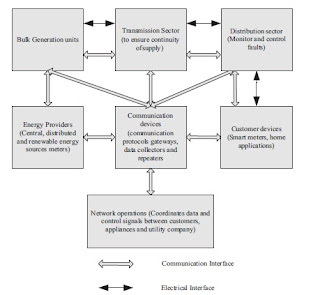
Figure below shows communication network for smart meter:


References:

1. Smart meters for power grid: Challenges, issues, advantages and status (Review Article) Renewable and Sustainable Energy ReviewsVolume 15, Issue 6August 2011Pages 2736-2742 Soma Shekara Sreenadh Reddy Depuru, Lingfeng Wang, Vijay Devabhaktuni

2. Koay BS, Cheah SS, Sng YH, Chong PHJ, Shum P, Tong YC, et al. Design and implementation of bluetooth energy meter. In: Proc. Fourth International Conference on Information, Communications & Signal Processing. 2003. p. 1474–7.