Friday, 15 March 2013

7 Segment Display Interfacing with 8051


INTRODUCTION: 

This post is about to interface a seven segment LED display to an 8051 microcontroller. Seven segment LED display is very popular and it’s just 7 LEDs that have been combined into one case to make a convenient device for displaying numbers and some letters. Knowledge about how to interface a seven segment display to a microcontroller is very helpful in designing embedded systems. A seven segment display consists of seven LEDs arranged in the form of a “squarish eight” slightly inclined to the right and a single LED as the dot character. Different characters can be displayed by selectively glowing the required LED segments. 

Seven segment displays are of two types, 

Common Cathode: In this method, all segment share common cathode. 

Common Anode: In this method, all segment share common anode. 

Here common anode seven segment display is used because the output current of the microcontroller is not sufficient enough to drive the LED’s. In order to turn ON a segment the corresponding pin must be set to 0 and to turn it OFF it is set to 1. 


A resistor is required to limit the current. Rather than using a resistor from each LED to ground, you can just use one resistor from Vcc to pin 3 (‘com’) to limit the current. 

DIGIT DRIVE PATTERN

Digit drive pattern of a seven segment LED display is simply the different logic combinations of its seven segment terminals ‘a’ to ‘h’ in order to display different digits and characters. The common patterns (0 to 9) of a seven segment display are shown in the table below. 


CIRCUIT DIAGRAM


INTERFACING CODE

// Programming for interfacing of Seven Segment Display to 8051 

#include<reg51.h> 

delay_ms(int time) // Time delay function 
int i,j; 
for(i=0;i<time;i++) 
for(j=0;j<1275;j++); 
void main() 
char num[]={0x40,0xF9,0x24,0x30,0x19,0x12,0x02,0xF8,0x00,0x10}; 
// Hex values corresponding to digits 0 to 9 
int s; 
while(1) 
    { 
    for(s=0;s<10;s++) 
        { 
          P2=num[s]; 
         delay_ms(200); 
        } 
    } 
}

Wednesday, 13 March 2013

LED Interfacing with 8051

-->

LED (LIGHT EMITTING DIODE) 

Light Emitting Diodes (LED) is the most commonly used electronic components, generally for display digital states. Typical uses of LEDs include alarm devices, timers and confirmation of user input such as a mouse click or keystroke, events etc. LEDs are very cheap and easily available in a variety of shape, size and colors. 

OPERATION OF LED: 

The principle of operation of LEDs is simple. 

When using an LED you must use a resistor to limit the current flow. If you just connect an LED directly to a pin of the micro controller you run the risk of damaging the micro controller by allowing too much current flow into or out of the pin. 

You have to be aware of the current limits for the pin at which you are going to connect LED. A port current limit is the total current flowing from a number of individual pins. 

Sinking (power flow into the pin) and sourcing (power flow out of the pin) may have slightly different current limits so you have to check the data sheet for the exact values. 

You can use 10-15 mA as a safe LED current which will provide decent light intensity and conserve battery power. 

Determine the Series resistor using Ohms law with an excess voltage value and current value for LED. 

Red LED's generally need 1.5V to 1.9V to light any extra voltage must be dropped with a series resistor else the LED will draw extra current in an attempt to lower the supply voltage down to the 1.5V level. 

The typical supply voltage is 5V. Then, 5 - 1.7 = 3.3V of excess voltage. 

Let’s design the LED to use 10mA 

Ohms law Resistance R = V / I 

3.3 / 10mA = 330 Ohms, Place a 330 ohm resistor in series with the LED. 

You can connect the LED and its resistor in one of two ways: 


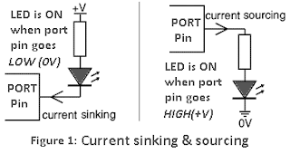
Sinking Current where the LED is connected to Positive power and the pin on the micro goes low to ground potential to light the LED. 

Sourcing Current the LED is connected to ground and the Pin on the micro controller goes HIGH to positive voltage to light the LED.

CIRCUIT DIAGRAM:


INTERFACING CODE:

             // Program to blink the LEDs (LEDs are connected to port 2)

#include<reg51.h>

void delay(int time)                               //This function produces a delay in msec.
{
int j,k;
for(j=0;j<time;j++)
for(k=0;k<1275;k++);
}
void main()
{
   while(1)
      {
        P2=0x00;
       delay(30);
       P2=0xff;
       delay(30);
      }
}
-->

Monday, 11 March 2013

AT Commands for GSM SIM 300 Interfacing


AT Commands are Instructions and used for control a Modem. Every command line start with "AT". That's why modem commands are called AT commands.
This article describes the AT commands for reading, sending and deleting SMS and also receiving, dialing, hanging a CALL from the SIM300 GSM modem inbox. You can also check the balance in sim card in SIM300.

Setup testing procedure for AT commands:

  • Insert the SIMCARD into SIM Tray
  • Connect the RS232 cable to the PC serial port (DB-9)
  • Open hyper terminal from windows 
  • Select the COM port with baud rate 9600 
  • Type AT commands and press enter and you will get OK; that means communication is OK.

Reading a SMS from the Inbox:

AT+CMGF=1 then press enter
AT+CMGR= no. and press enter; Number (no.) is the message index number stored in the SIM card.
The modem will reply with the text of the first SMS in the inbox along with sender’s mobile number, date and time.

Sending SMS from SIM300:

AT+CMGF=1 press enter
AT+CMGS=”mobile number” press enter
Once The AT commands is given’ >’ prompt will be displayed on the screen.
Type the message to send via SMS. After this, press ctrl+Z to send the SMS.
If the SMS sending is successful, “ok” will be displayed along with the message number.

Deleting a SMS from inbox:

  • To delete the first message from the inbox type the command AT+CMGD=1 and press enter; the modem will delete the first message in the inbox. 
  • To delete the second message from the inbox type the command AT+CMGD=2 and press enter; the modem will delete the second message in the inbox …..and so on. 

Receiving an incoming Call:

To receive a ringing call, type the command ATA and press enter

Dialing a new number from SIM300:

To call to a number send the command ATD followed by the mobile number
For example, to call the mobile number 9928142466 send the command as, ATD9928142466; and press enter

Hanging up a call:

To hang up a ringing call or a call in progress type the command ATH and press enter

How to check a balance in SIM300?

To check a balance in your simcard in SIM300 type the command ATD followed by your service provider balance checking number; For example to check balance for Airtel or BSNL; type ATD*123# and press enter, You will get your simcard balance with expire date.


Interfacing 16x2 LCD with 8051

-->

LCD display is an inevitable part in almost all embedded applications and this article is about interfacing 16×2 LCD with 8051 Microcontroller. Many guys find it hard to interface LCD module with the 8051 but the fact is that if you learn it properly, it’s a very easy job and by knowing it you can easily design embedded display applications. Thoroughly going through this article will make you able to display any text (including the extended characters) on any part of the 16×2 display screen. In order to understand the interfacing first you have to know about the LCD.


What is 16×2 LCD Module?

16×2 LCD module is a very common type of LCD module that is used in 8051 based embedded applications. It consists of 16 rows and 2 columns of 5×7 or 5×8 LCD dot matrices. The module were are talking about here is type number JHD 162A which is a very popular one. It is available in a 16 pin package with back light, contrast adjustment function and each dot matrix has 5×8 dot resolution. The pin numbers, their name and corresponding functions are shown in the table below. 

Pin No. Name  Function
  1.   Vss        This pin must be connected to the ground 
  2.   VCC       Positive supply voltage pin (+5V DC) 
  3.   VEE       Contrast adjustment 
  4.   RS         Register selection 
  5.   R/W       Read or write 
  6.   E           Enable 
  7.   DB0       Data 
  8.   DB1       Data 
  9.   DB2       Data 
  10.   DB3       Data 
  11.   DB4       Data 
  12.   DB5       Data 
  13.   DB6       Data 
  14.   DB7       Data 
  15.   LED+     Back light LED+ 
  16.   LED-      Back light LED- 
VEE pin is meant for adjusting the contrast of the LCD display and the contrast can be adjusted by varying the voltage at this pin. This is done by connecting one end of a POT to the Vcc (5V), other end to the Ground and connecting the center terminal (wiper) of the POT to the VEE pin. See the circuit diagram for better understanding.

The JHD 162A has two built in registers namely data register and command register. Data register is for placing the data to be displayed, and the command register is to place the commands. The 16×2 LCD module has a set of commands each meant for doing a particular job with the display. We will discuss in detail about the commands later. High logic at the RS pin will select the data register and Low logic at the RS pin will select the command register. If we make the RS pin high and the put a data in the 8 bit data line (DB0 to DB7), the LCD module will recognize it as a data to be displayed. If we make RS pin low and put a data on the data line, the module will recognize it as a command. 

R/W pin is meant for selecting between read and write modes. High level at this pin enables read mode and low level at this pin enables write mode.

E pin is for enabling the module. A high to low transition at this pin will enable the module. 

DB0 to DB7 are the data pins. The data to be displayed and the command instructions are placed on these pins. 

LED+ is the anode of the back light LED and this pin must be connected to Vcc through a suitable series current limiting resistor. LED- is the cathode of the back light LED and this pin must be connected to ground. 


What is 16×2 LCD Commands? 

16×2 LCD module has a set of preset command instructions. Each command will make the module to do a particular task. The commonly used commands and their function are given in the table below. 

LCD Command Function 

0F      LCD ON, Cursor ON, Cursor blinking ON 
01      Clear screen 
2         Return home 
4         Decrement cursor 
06       Increment cursor 
E        Display ON, Cursor ON 
80       Force cursor to the beginning of 1st line 
C0      Force cursor to the beginning of 2nd line 
38      Use 2 lines and 5×7 matrix 
83      Cursor line 1 position 3 
3C     Activate second line 
0C3    Jump to second line, position3 
OC1   Jump to second line, position1 


LCD initialization 

The steps that have to be done for initializing the LCD display is given below and these steps are common for almost all applications. 
  • Send 38H to the 8 bit data line for initialization
  • Send 0FH for making LCD ON, cursor ON and cursor blinking ON.
  • Send 06H for incrementing cursor position.
  • Send 01H for clearing the display and return the cursor.

Sending data to the LCD 

The step for sending data to the LCD module is given below. I have already said that the LCD module has pins namely RS, R/W and E. It is the logic state of these pins that make the module to determine whether a given data input is a command or data to be displayed. 
  • Make R/W low.
  • Make RS=0 if data byte is a command and make RS=1 if the data byte is a data to be displayed.
  • Place data byte on the data register.
  • Pulse E from high to low.
  • Repeat above steps for sending another data.

Circuit


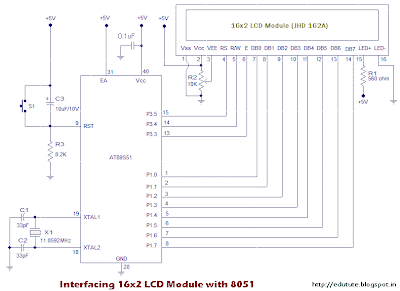
The circuit diagram given above shows how to interface a 16×2 LCD module with AT89S1 microcontroller. Capacitor C3, resistor R3 and push button switch S1 forms the reset circuitry. Ceramic capacitors C1, C2 and crystal X1 is related to the clock circuitry which produces the system clock frequency. P1.0 to P1.7 pins of the microcontroller is connected to the DB0 to DB7 pins of the module respectively and through this route the data goes to the LCD module. P3.3, P3.4 and P3.5 are connected to the E, R/W, RS pins of the microcontroller and through this route the control signals are transferred to the LCD module. Resistor R1 limits the current through the back light LED and so do the back light intensity. POT R2 is used for adjusting the contrast of the display. 


Assembly Program 

MOV A,#38H // Use 2 lines and 5x7 matrix 
ACALL CMND 
MOV A,#0FH // LCD ON, cursor ON, cursor blinking ON 
ACALL CMND 
MOV A,#01H //Clear screen 
ACALL CMND 
MOV A,#06H //Increment cursor 
ACALL CMND 
MOV A,#82H //Cursor line one , position 2 
ACALL CMND 
MOV A,#3CH //Activate second line 
ACALL CMND 
MOV A,#49D 
ACALL DISP 
MOV A,#54D 
ACALL DISP 
MOV A,#88D 
ACALL DISP 
MOV A,#50D 
ACALL DISP 
MOV A,#32D 
ACALL DISP 
MOV A,#76D 
ACALL DISP 
MOV A,#67D 
ACALL DISP 
MOV A,#68D 
ACALL DISP 
MOV A,#0C1H //Jump to second line, position 1 
ACALL CMND 
MOV A,#67D 
ACALL DISP 
MOV A,#73D 
ACALL DISP 
MOV A,#82D 
ACALL DISP 
MOV A,#67D 
ACALL DISP 
MOV A,#85D 
ACALL DISP 
MOV A,#73D 
ACALL DISP 
MOV A,#84D 
ACALL DISP 
MOV A,#83D 
ACALL DISP 
MOV A,#84D 
ACALL DISP 
MOV A,#79D 
ACALL DISP 
MOV A,#68D 
ACALL DISP 
MOV A,#65D 
ACALL DISP 
MOV A,#89D 
ACALL DISP 
HERE: SJMP HERE 
CMND: MOV P1, A 
CLR P3.5 
CLR P3.4 
SETB P3.3 
CLR P3.3 
ACALL DELY 
RET; 
DISP: MOV P1, A 
SETB P3.5 
CLR P3.4 
SETB P3.3 
CLR P3.3 
ACALL DELY 
RET; 
DELY: CLR P3.3 
CLR P3.5 
SETB P3.4 
MOV P1, #0FFh 
SETB P3.3 
MOV A, P1 
JB ACC.7, DELY 
CLR P3.3 
CLR P3.4 
RET; 
END

Subroutine CMND sets the logic of the RS, R/W, E pins of the LCD module so that the module recognizes the input data (given to DB0 to DB7) as a command. 

Subroutine DISP sets the logic of the RS, R/W, E pins of the module so that the module recognizes the input data as a data to be displayed.
-->

Sunday, 10 March 2013

What is PCB (Printed Circuit Board) ?

-->
Definition:
A PCB is a Printed Circuit Board, and used to mechanically support and electrically connect electronic components using conductive pathways (copper traces), signal traces etched from copper sheets laminated onto a non-conductive substrate Glass Epoxy (FR4).

Also PCBs are a composite of organic and/or inorganic dielectric materials with many layers with wiring interconnects and also house components like inductors and capacitors. There isn’t any standard printed circuit board as such and each board is unique, often a function of the product itself.

PCB Design Layers:


A PCB design package allows the designer to define and design on multiple layers.

Many of these are physical layers such as:
• Signal Layer
• Power plane Layer
• Mechanical Layer

And some are special layers such as:
• Solder & Paste Mask Layers
• Silkscreen or Top Overlay Layers
• Drill guides
• Keep-out Layer

Types of PCB:

A PCB can be of four types: Rigid board , Flexible board and Rigid-flex board, Metal-core and Injection Molded boards out of which the Rigid board is the most popular. Further these may be Single Sided, Double Sided or Multilayer. 
The mechanical, electrical, chemical and thermal properties of the material should be considered while making PCBs otherwise the reliability of the board suffers. Presently, copper-clad laminates of different reinforced resin systems are used in rigid boards. Examples include Fire resistant FR-4 epoxies, PTFE, cyanate esters, polymides etc. Most commonly used reinforcement material is continuous filament E-Glass. Flexible and rigid flex-boards have random arrangements of conductors on a flexible base and may be with/without cover layers. Here, the wiring is restricted to select areas of the plane. In case of constraining metal core technology, the PCB can be of standard materials but the core materials must have low Coefficient of Thermal Expansion and strength to constrain the PCB. Copper-Invar-Copper and Copper-Molybdenum-Copper are two popular materials for this purpose. Molded boards have resins containing fillers which are molded into a die to form the required shapes.

What is PCB Board Design?


  • PCB board design defines the electrical pathways between components
  • It is derived from a schematic representation of the circuit
  • When it is derived, or imported from a schematic design, it translates the schematic symbols and libraries into physical components and connections


PCB Manufacturing Process:


Step 1: Film Generation

The film is generated from the design files (Gerber/CAM files) which are sent to the manufacturing house. One film is generated per layer

Step 2: Raw Material

Industry standard 0.059” thick, copper clad panel

Step 3: Drill Holes

Using NC machines and carbide drills to drill holes according to the drill spec sent to the manufacturing house

Step 4: Electroless Copper

Apply thin copper deposit in hole barrels

Step 5: Apply Image

Apply photosensitive dry film to panel and use a light source and the film to expose the panel

Step 6: Pattern Plate

Electrochemical process to build copper in the holes and on the trace areas. Apply tin to surface

Step 7: Strip and Etch

Remove the dry film, and then etch the exposed copper. The tin protects the copper circuitry from being etched away

Step 8: Solder Mask

Apply a solder mask area to the entire board with the exception of solder pads

Step 9: Solder Coating

Apply solder to pads by immersing into tank of solder. Hot air knives level the solder when removed from the tank

Step 10: Nomenclature(Silk Screen Printing)

Apply white letter markings using screen printing process
-->

In System Programming


For embedded system application you have a dedicated intelligent semiconductor chip which is capable to execute a software program, and behave at input and output data pins as per software instructions. These chips are called a processor and a processor can be microcontroller, microprocessor, DSP, etc. 
The software for such embedded system processor generally is written in the laptop or PC, compiled (or assembled) using a cross-compiler tool (called cross compiler because program is written in PC and executed in embedded processor). Compiler (or assembler) generate executable file for the particular processor and this program should be inserted (saved) in processor's non-volatile memory (internal or external). 


Programming the processors's nonvolatile memory is itself a tough task. In earlier days practice was to remove processors or its external memory from target board and place it in a specific programming device. Even today many people program processor in same way. But a new and convenient way is to program the processor or its memory while remaining in the target board. It is called in system programming. 

What you need for in system programming?

  1. Hardware interface from you PC, so that the executable program can be transferred from PC / Laptop. This interface can be DB-9 connector, USB or parallel (printer) port. 
  2. Software running in the PC which can control the data sending on hardware interface port. Generally this software are Flash tools like Flash magic, or IDEs like TI's code composer studio, Microchip's MPLAB, etc
  3. A specific hardware which would recieve data from the PC and transfer it to target board using a special hardware interface like SPI (serial programming interface), JTAG, Microchip's ICD, etc. Here JTAG and ICD have additional capability for debugging. 
  4. Sometime, the hardware interface mentioned in last point is not used. But the target processor itself have BOOTLOADER software programmed or pre-programmed in it. Bootloader is a software in the program memory executes when processor resets. It give use a option to either run the existing application software or receive a new application software from PC using a serial interface. Generally PC transfer data using RS-232 (DB-9 connector) and MAX 232 IC convert it to UART (Rx, Tx) data. This self programming capablity using boot loader provides excellent convenience and low cost. But it need a boot loader in the processor and UART compability.